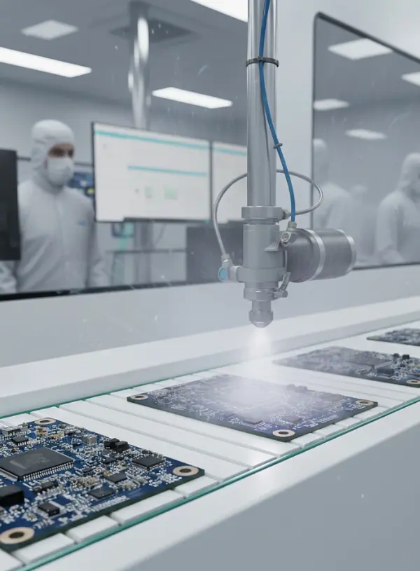
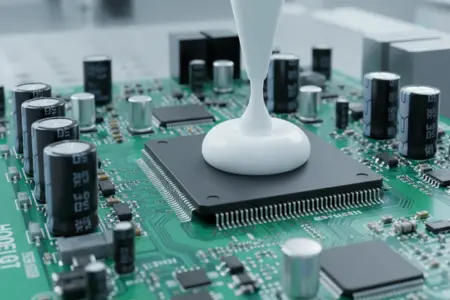
Conformal Coating that Sticks on PCBs
Improving wettability and adhesion for urethane, acrylic, or silicone conformal coatings using inline plasma treatment right before dispense or dip.
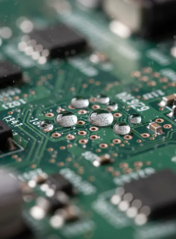
Every electronics manufacturer knows the frustration when they’ve applied a protective conformal coating to PCBs, only to find it peeling at the edges, forming voids around components, or developing bubbles that trap moisture. These are pathways to corrosion, electrical failures, and warranty claims that can cost thousands per batch.
The root cause is usually poor surface adhesion. Your coating might be world-class, but if it can't properly wet and bond to the PCB surface, it's not protecting anything. It's just expensive chemistry waiting to fail.
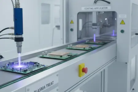
Here's what changes when you add inline atmospheric plasma treatment immediately before your coating process:
Surface energy jumps from problematic 30-35 dynes/cm to a robust 45-50 dynes/cm.
Coatings flow smoothly into tight spaces.
Adhesion test results become boringly consistent.
Field failures drop to near zero.
If you don’t want to learn about this and you just want the plasma treater we built to help conformal coatings stick on PCBs, you can submit for a quote in 20 seconds.
Why Do Conformal Coatings Sometimes Fail to Adhere to PCB Surfaces?
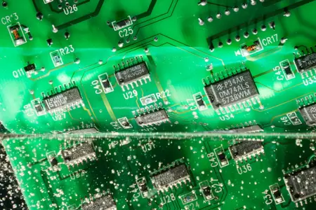
PCBs present a perfect storm of adhesion challenges.
Start with the substrate itself - FR4 epoxy glass has reasonably good surface energy, but that's just the beginning of your problems.
Solder mask creates low-energy zones that actively repel coatings. The smooth, glossy finish that looks so professional? It's also chemically inert, offering few bonding sites for your coating molecules. Surface energy typically measures 28-32 dynes/cm - well below the 40+ dynes/cm threshold needed for reliable wetting.
Then there's contamination. Even after cleaning, PCBs harbor invisible enemies of adhesion.
Flux residues that create hydrophobic patches.
Fingerprints from handling (yes, even with gloves).
Mold release agents from plastic components.
Oxidation on exposed copper traces.
Silicone contamination from assembly areas.
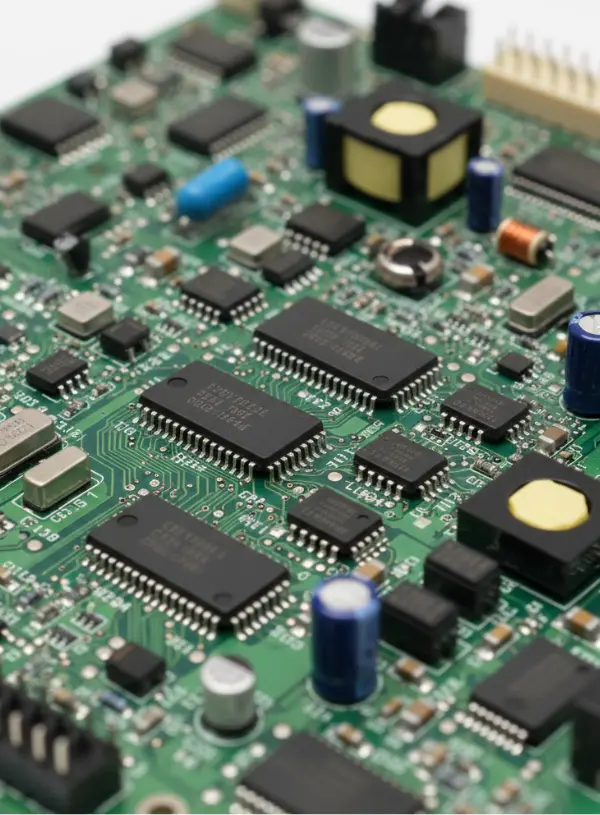
Mixed materials compound the problem. A single board might include FR4 substrate, copper traces, tin-lead or lead-free solder, various plastic connectors, and metallic shields. Each material has different surface energy. Your coating needs to adhere equally well to all of them, or you get selective delamination - protection exactly where you don't need it, gaps exactly where you do.
How Does Plasma Treatment Improve Coating Wetting on Complex PCB Assemblies?
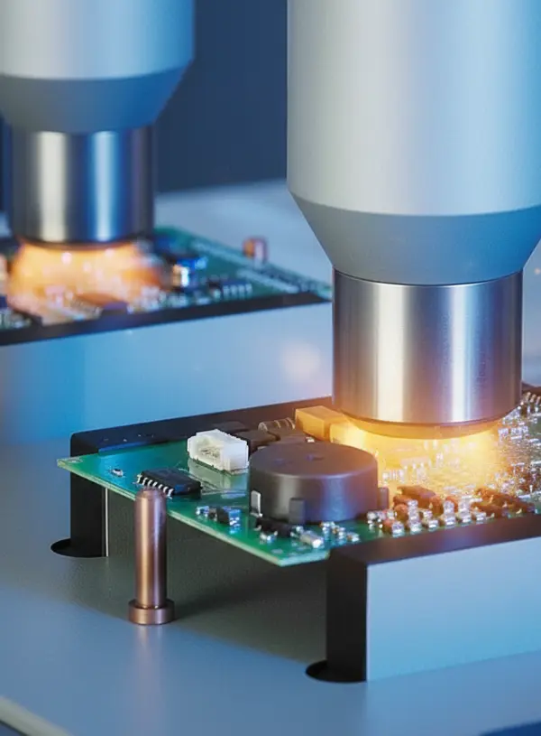
Atmospheric plasma alters surface chemistry at the molecular level. The ionized gas stream breaks existing bonds and introduces polar functional groups - primarily hydroxyl (-OH) and carbonyl (C=O) groups. These act like molecular velcro for coating adhesion.
The transformation happens in seconds. Low-energy surfaces become high-energy surfaces. Hydrophobic zones turn hydrophilic. Your urethane, acrylic, or silicone coating suddenly finds a surface it recognizes and can bond with chemically, not just mechanically.
But plasma does more than just activate. It performs micro-cleaning simultaneously, breaking down and volatilizing organic contaminants that survived your cleaning process. That stubborn flux residue? Vaporized. The invisible fingerprint? Gone. The result is a uniformly clean, uniformly activated surface ready for coating.
The treatment works across all those mixed materials on your PCB. Plasma doesn't care if it's treating solder mask, bare FR4, or plastic connectors. Each surface gets functionalized appropriately, creating consistent wettability across the entire assembly.
Get a quote for your application here
Which Coating Chemistries Benefit Most from Plasma Pretreatment?
Different conformal coatings respond differently to plasma activation, but all show improvement.
Acrylic coatings see the most dramatic benefits. These fast-drying, reworkable coatings often struggle with adhesion on low-energy surfaces. Plasma treatment eliminates the beading and crawling that plague acrylic applications, especially around fine-pitch components where coating thickness matters.
Urethane coatings gain improved chemical bonding. While urethanes generally have better inherent adhesion than acrylics, plasma treatment ensures complete coverage in shadow areas and under components where capillary action needs help. The enhanced wetting reduces void formation - those tiny gaps that become moisture ingress points.
Silicone coatings, despite their flexibility and wide temperature range, are notorious for dewetting on contaminated surfaces. Plasma treatment gives silicones the clean, activated surface they need for proper flow and adhesion. This is especially critical for thick silicone applications where gravity works against you.
Parylene coatings benefit during the pre-deposition phase. While Parylene is vapor-deposited rather than liquid-applied, plasma pretreatment improves the initial nucleation and growth, resulting in better adhesion and fewer pinholes.
Even UV-cure coatings show improved performance after plasma treatment. The enhanced surface energy ensures better initial flow before curing, reducing the orange-peel effect and improving overall coverage uniformity.
How Much Surface Energy Increase Is Needed for Reliable Conformal Coating?
The magic number for most conformal coatings is 40 dynes/cm minimum. Below this threshold, you're fighting physics. Above it, coatings wet properly, flow into tight spaces, and form durable chemical bonds.
Untreated PCB surfaces typically measure:
Solder mask: 28-32 dynes/cm.
FR4 (clean): 35-38 dynes/cm.
Plastic connectors: 30-34 dynes/cm.
Flux residues: 25-30 dynes/cm.
After plasma treatment, these same surfaces achieve:
All surfaces: 42-50 dynes/cm uniformly.
This creates a comfortable margin above minimum requirements. That buffer matters when you factor in normal production variables like humidity, temperature fluctuations, and minor contamination.
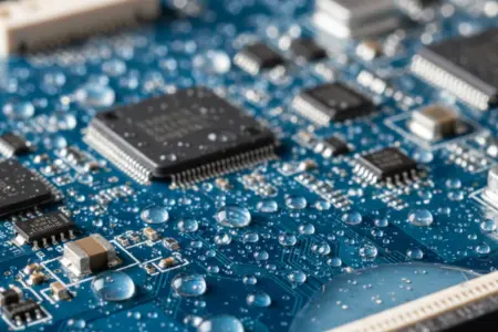
Verification takes seconds with dyne test pens or contact angle measurement. Water droplet contact angles drop from 80-90° on untreated surfaces to 20-30° after plasma treatment. That's the difference between water beading up versus spreading flat - exactly what you want your coating to do.

Does Plasma Treatment Damage Sensitive PCB Components During Processing?
This concern comes up in every implementation discussion.
The good news is that properly controlled atmospheric plasma treatment poses no risk to electronic components.
The treatment is entirely non-contact. The plasma field extends only 5-20mm from the treatment head, and the ionized gas stream doesn't generate significant heat at the substrate level. Component temperatures might rise 5-10°C during treatment - less than they experience during reflow soldering.
No electromagnetic interference affects sensitive circuits. The plasma operates at atmospheric pressure using low-frequency excitation that doesn't induce currents in PCB traces. It's gentler than the static discharge your boards experience during normal handling.
Fine-pitch components, BGAs, and even exposed die remain unaffected. The treatment intensity is adjustable - you can dial in exactly the activation level needed without over-treating. Yamato's programmable controls let you create recipes for different board types, ensuring consistent treatment without risk.
For ultimate protection of specific areas, simple masking works. But most applications don't need it. The plasma treatment is selective to organic surfaces - it won't affect gold contacts, won't degrade solder joints, and won't impact component markings.
Why Choose Plasma Treatment Instead of Chemical Adhesion Promoters?
Chemical adhesion promoters have been the default solution for decades. They work, but you wouldn’t be reading this if you were satisfied.
Consider what primers and adhesion promoters actually bring to your process…

Consumable costs that never end - typically $50-200 per gallon.

VOC emissions requiring ventilation and permits.

Hazardous waste disposal for used solvents and contaminated materials.

Process time for application and flash-off.

Inconsistent application leading to variable results.

Storage requirements for flammable materials.

Worker exposure risks requiring PPE and monitoring.
Plasma treatment eliminates all of these. The only consumables are electricity and compressed air. No VOCs, no hazardous waste, no storage headaches. The treatment happens in seconds with perfect consistency, batch after batch.
A typical PCB line using adhesion promoters generates 500-1000 pounds of hazardous waste annually. A plasma system generates zero chemical waste. In states with strict environmental regulations, this alone can justify the investment.
How Long Does the Plasma-Treated PCB Surface Remain Active for Coating?
Surface activation from plasma treatment isn't permanent, but it lasts plenty long for practical production needs. The activated surface maintains optimal coating receptivity for:
First 30 minutes: Maximum adhesion potential.
30 minutes to 2 hours: Excellent adhesion.
2 to 8 hours: Good adhesion.
Beyond 8 hours: Degraded but still improved versus untreated.
These timeframes assume normal cleanroom conditions. High humidity accelerates hydrophobic recovery. Contamination from handling or airborne particles can reduce the window. But here's why timing rarely becomes an issue: inline integration.
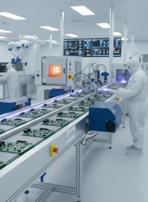
When your plasma treater sits immediately upstream of your coating station, treatment-to-coating time measures in seconds, not hours. The board gets treated, moves 12 inches, and gets coated. No degradation, no contamination, no variables.
For batch operations where boards must be treated and stored, simple precautions extend the activation window. Store in clean, dry conditions. Use static-dissipative bags. Minimize handling. Even then, you're working with hours of viable activation time - more than enough for most production scenarios.
Get your plasma treater quote within 48 hours
Can Plasma Treatment Replace Manual PCB Cleaning Steps?
Plasma treatment excels at micro-cleaning but doesn't replace gross contamination removal. Think of it as the finishing step that ensures coating success, not a substitute for proper board preparation.
- Light organic films and residues.
- Fingerprints and handling contamination.
- Trace flux residues after aqueous cleaning.
- Mold release agents from plastic components.
- Surface oxidation on exposed metals.
- Heavy flux deposits.
- Visible contamination or debris.
- Thick organic films.
- Ionic contamination requiring extraction.
The real value comes from using plasma as a complement to your existing cleaning process. You might be able to eliminate a final solvent wipe. You can definitely eliminate adhesion promoters. Some operations successfully replace IPA wipe-downs with plasma treatment, saving thousands in solvent costs annually.
How Can You Verify Coating Adhesion After Plasma Treatment?
Documentation beats hope every time. Proper verification protocols protect you from field failures and warranty claims.
Immediate verification methods:
- Dyne pen testing: Quick go/no-go surface energy confirmation.
- Contact angle measurement: Quantitative wettability data.
- Test coupons: Run sample boards alongside production.
Post-coating adhesion tests:
- Cross-hatch adhesion (IPC-CC-830 / ASTM D3359): Industry standard for coating adhesion.
- Tape pull tests: Quick production floor verification.
- Thermal shock testing: Coating adhesion after temperature cycling.
Long-term reliability testing:
- Salt fog exposure (ASTM B117): Corrosion resistance validation.
- Temperature/humidity cycling: Real-world environmental simulation.
- Dielectric withstand voltage: Ensuring insulation integrity.
The beauty of plasma treatment is the consistency. Once you dial in parameters that pass your adhesion tests, those results reproduce shift after shift. No more wondering if the operator mixed the adhesion promoter correctly or if humidity affected your primer application.
What Production Throughput Can Atmospheric Plasma Systems Handle?
Plasma treatment scales with your production needs. The treatment head width adjusts from 20mm for single boards to 400mm+ for panel processing. Line speeds from 0.5 to 20 meters per minute are achievable depending on activation requirements.
For typical PCB conformal coating lines:
Small boards (cell phones, wearables): 30-60 units per minute.
Small boards (cell phones, wearables): 30-60 units per minute.
Large boards (server motherboards): 5-10 units per minute.
Panel processing: 2-5 panels per minute.
Your Yamato plasma treater integrates with existing conveyors, maintaining your current line speed without bottlenecks. Multiple treatment heads can work in parallel for wider boards or faster processing. The instant on/off capability means no warmup time, no cooldown time - just consistent treatment whenever boards are present.
What's the Real ROI for PCB Manufacturers Using Plasma Pretreatment?
The financial case for plasma treatment builds from multiple savings streams.
Direct cost reductions:
- Eliminate adhesion promoters: tens of thousands of dollars annually in chemicals.
- Reduce rework: 2-5% typical reduction in coating defects.
- Cut disposal costs: No hazardous waste from primers.
- Lower labor: No primer application or flash-off time.
Post-coating adhesion tests:
- Fewer field failures reducing warranty costs.
- Improved first-pass yield increasing throughput.
- Simplified environmental compliance and reporting.
- Reduced inventory (no primer storage).
A typical mid-size PCB assembly operation sees payback in 6-12 months. High-reliability sectors (medical, aerospace, automotive) often justify the investment on warranty cost avoidance alone - one prevented field failure can offset months of operational costs.
How to Integrate Plasma Treatment into Your Existing Conformal Coating Line?
Implementation follows a logical sequence that minimizes disruption:
Week 1-2: Validation
- Test your specific PCB types and coatings.
- Establish optimal treatment parameters.
- Document adhesion improvements.
Week 3-4: Integration
- Install inline between final inspection and coating.
- Set working distance (typically 10-15mm).
- Program treatment recipes for different board types.
- Validate with production volumes.
Week 5-6: Optimization
- Fine-tune for maximum line speed.
- Train operators on verification methods.
- Establish quality control protocols.
The compact footprint of Yamato's plasma treater means most installations require no line reconfiguration. Mount it on your existing conveyor, connect power and compressed air, and you're treating boards within hours.
What Are Common Troubleshooting Solutions for PCB Plasma Treatment?
Even robust processes need occasional adjustment. Here's how to address common challenges.
Uneven treatment across board width?
- Verify consistent gap between treatment head and PCB surface.
- Check for board warpage causing distance variations.
- Adjust treatment width to ensure full coverage with overlap.
Some components showing reduced adhesion?
- Shadow effects from tall components may require angle adjustment.
- Increase treatment intensity for boards with mixed materials.
- Consider dual-pass treatment for complex assemblies.
Treatment effect seems to fade quickly?
- Minimize time between treatment and coating.
- Check storage environment for contamination sources.
- Verify compressed air quality (oil-free, dry).
Coating still showing some dewetting?
- Increase treatment intensity or reduce line speed.
- Verify no silicone contamination in environment.
- Check coating viscosity and application parameters.
The compact footprint of Yamato's plasma treater means most installations require no line reconfiguration. Mount it on your existing conveyor, connect power and compressed air, and you're treating boards within hours.
Why This Matters The Bigger Picture for PCB Reliability
Conformal coating protects the billions of dollars of electronics that run our world. When coatings fail, systems fail. Cars strand drivers. Medical devices alarm unnecessarily. Industrial controls shut down production lines.
Atmospheric plasma treatment transforms coating adhesion from a variable you worry about to a constant you control. No more chemistry roulette with adhesion promoters. No more crossing fingers during salt fog testing. Just consistent, measurable, reproducible surface activation that ensures your protective coatings actually protect.
For PCB manufacturers committed to reliability, the question isn't whether to implement plasma treatment - it's how quickly you can integrate it. Every board that ships with questionable coating adhesion is a warranty claim waiting to happen. Every rework cycle for coating defects is profit walking out the door.
Yamato's atmospheric plasma treater delivers the precision, consistency, and integration simplicity that modern PCB manufacturing demands. Built on 136 years of Japanese engineering excellence and Kaizen principles, it's designed to run shift after shift, year after year, keeping your coatings stuck and your electronics protected.
Ready to eliminate coating adhesion failures from your PCB production? Contact us for application-specific testing with your boards and coatings. See the difference proper surface activation makes - first board, every board.