Physics is no one’s friend at a chip fab, especially not at advanced nodes and in the most advanced 2.5D and 3D-IC packages. As we push the boundaries with increasing density, smaller features, and thinner dies, we face a paradox. These advancements make heat dissipation increasingly difficult, ramping up mechanical stress, while simultaneously making it harder to insulate and protect against this very heat.
The result? A heightened risk of thermal runaway or accelerated aging, and a higher propensity for failure. That is a loss of yield for those who are managing deployment.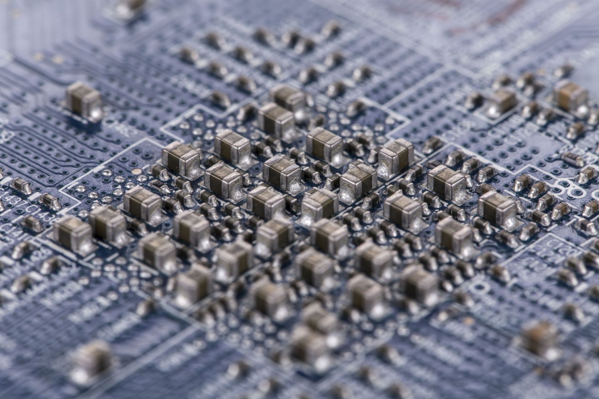
How do we tackle these thermal challenges?
The key lies in material selection. Each package configuration may require a unique optimum configuration that balances competing requirements, like flexibility versus thermal conductivity. This complexity is amplified in heterogeneous designs. Here, diverse materials, each with its own coefficient of thermal expansion, can lead to die shift, warpage, and connection failures. These issues don't just impact the integrity of the design; they can also have profound effects on performance and power efficiency. Therefore, addressing thermal effects is about early identification, thorough analysis, and proactive solutions.
Enter the first and only analyzer for accurate thermal data of packaging substrates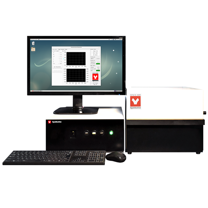
Here’s how it works:
- Prepare your sample substrate by attaching a TEG Chip to simulate next-generation power devices in driving mode
- Place the prepared sample on a water-cooled heat sink
- Attach the power supply to TEG chip and heat up
- Find the temperature difference (ΔT) between the registered temperature of the TEG chip and the heat sink
- Calculate the thermal resistance value(Rth) of the sample substrate
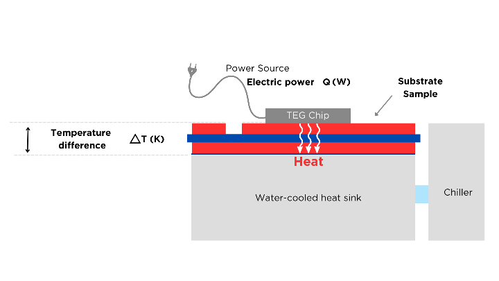
Thermal resistance (Rth) = Temperature difference (ΔT) between TEG chip and heat sink, divided by electric power (Q)
Do I have a big enough package?
The semiconductor industry has always handled architecture questions relying on budgeting and approximate models.
However, it's unrealistic to expect a single material set to work universally across various package types and sizes. Moreover, advanced packaging often involves mixing and matching materials that have been modified specifically to add a mechanical margin to counteract stress, like silicon nitride, aluminum nitrate, alumina, etc.
What this new workflow with our patented TE100 thermal analyzer gives you is data for precise thermal budgeting and a conclusive understanding of how different substrate materials and configurations will behave under actual operational conditions. This level of analysis is crucial for addressing the complex thermal dynamics in advanced semiconductor packaging at the design stage, and ensuring your product reliability and maximizing yield during production.
How does it help me increase my yield?
Even the most meticulously planned designs aren't immune to thermal stresses during manufacturing – and the ways these stresses manifest can be unpredictable. In heterogeneous packages, where components have varying heat tolerances, this challenge becomes even more daunting as dimensions shrink.
Why?
#1. The entire manufacturing process is governed by temperature. Each processing step has its own thermal level, followed by a cool down to room temperature, creating a thermal contrast. This contrast can lead to latent defects, which might not be apparent immediately but can cause failures months or even years later. For instance, the routine of power cycling — the frequent powering on and off of a device — can induce fatigue failures that go unnoticed during initial processing stages. In some extreme cases, this heat can even cause entire PCBs to bend or warp.
#2. Adding to the complexity, predicting these latent defects is a formidable challenge. Analysis and inspection typically focus on the package level, not on the integration of the system as a whole. Therefore, even if a wafer passes initial inspections, there's no absolute assurance that it won't encounter failures at the package or system level due to a multitude of interacting factors.
Traditionally, the industry has relied on approximations and modeling to determine the ideal combination of materials, dimensions, and densities to minimize stress. However, these methods can fall short, as latent defects can still develop in the absence of noticeable stress at room temperature.
With the TE100, it's possible to test each substrate individually, measuring its thermal resistance value in real-time, in its actual working environment. This in-situ testing provides valuable data that can be used to inform the design and packaging of chips, offering a more accurate and comprehensive approach to managing thermal stresses. By incorporating this sophisticated testing into the manufacturing process, you can greatly enhance the predictability and reliability of semiconductor products, leading to an increase in yield and a reduction in the risk of unexpected failures post-manufacturing.
Sounds interesting? Chat with our consultants about setting up a demonstration to see the TE 100 in action.